Flip chip technology has its name by flipping over the chip to connect with the substrate. Unlike conventional interconnection through wire bonding, flip chip uses solder or gold bumps instead.
Therefore, the I/O pads can be distributed all over the surface of the chip, not only on the peripheral region. The chip size can be shrunk, and the circuit path can be optimized. Additionally, no bonding wire means no wire inductance.
The growth of low profile and high performance for high volume, non-traditional consumer application are driving the flip chip technology to replace the traditional wire-bond and TAB type interconnections.
Applications of Flip Chip Package
- Computing: MPU, chipset, graphic driver, high speed memory
- Consumer: cellular phone, pager, PDA, watch
- Communication: transmission, switching, cellular base stations
- Power management: power regulator
- RF / wireless networking: RF driver
- Others: programmable logic device
Flip Chip Package Application Map
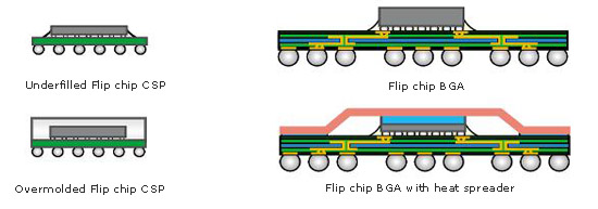
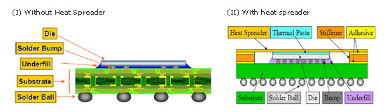
Cross Section of Flip Chip Package
UBM (Under Bump Metallurgy)
Solder bump is most common used for flip chip interconnection nowadays. UBM is the interface between final metal pad and solder bump, helping solder wet to the final metal pad. It is usually composed of several metal layers, which provide a number of functions including forming a solder- wettable surface, providing a diffusion barrier to intermetallic formation, preventing oxidization forming, with the following features.
- Good adhesive to the wafer passivation
- Good adhesive to the IC final metal pad
- Protection of the IC final pad from the environment
- Low resistance between IC final metal and solder bump
- An effective wettable metal of appropriate thickness
- Ability to be used on probed wafer
Successful Flip Chip Projects
Substrate stack-up and package side view
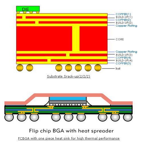
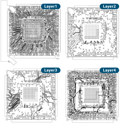
FCBGA substrate design example