Wafer Level Chip Scale Package refers to the technology of packaging an integrated circuit at the wafer level, instead of the traditional process of assembling individual units in packages after dicing them from a wafer. This process is basically an extension of the wafer Fab processes, where the device interconnects and protection are accomplished using the traditional fab processes and tools. In the final form, the device is essentially a die with an array pattern of bumps or solder balls attached at an I/O pitch that is compatible with traditional circuit board assembly processes. WLCSP is essentially a true chip-scale packaging (CSP) technology.
WLCSP technology differs from other ball-grid array (BGA) and laminate-based CSPs in that no bond wires or interposer connections are required. The key advantages of the WLCSP is the die to PCB inductance is minimized, reduced package size, and enhanced thermal conduction characteristics.
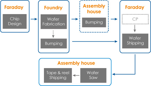
WLCSP Turnkey Service Flow
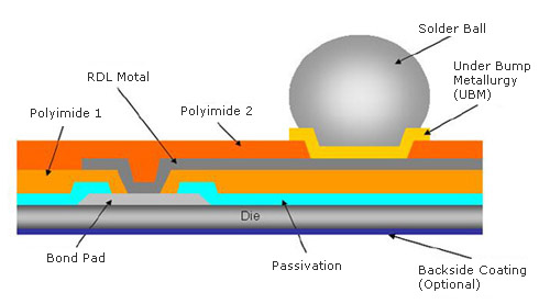
WLCSP Construction
Refer to the figure below for a representation of a typical WLCSP package with Redistribution Layer (RDL) and Under Bump Metallization (UBM) process. A WLCSP die has a first layer of organic dielectric (Polyimide 1), a metal redistribution layer (RDL) to re-route the signal path from the die peripheral I/O to a new desired location, and a second polyimide layer (Polyimide 2) to cover the RDL metal, which in turn is patterned into the solder ball array. To prevent diffusion and enable solder wetting, an under-bump metallization (UBM) layer is deposited on the RDL. The solder ball is a lead-free alloy. Backside wafer lamination, a protective polymer film, is optional for WLCSP productions. This polymer material offers both mechanical contact (i.e. SMT assembly pick and place) and UV light protection to the backside of the die surface.