Cu-pillar bumping is a next-generation flip chip interconnection between chip & packages (FCBGA/FCCSP), especially for fine pitch applications.


Why Cu-pillar Bump
On the wafer end, comparing to solder bump, cu-pillar bump provides the advantage of fine pitch; the die size can be reduced about 5~10%. On the package end, the substrate layer can be reduced from 6 layers to 4 layers by fine pitch and bump on trace process and using simplified substrate process. Therefore, the substrate cost declines about 30%.

Cu-Pillar Bump + FCCSP
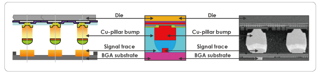
Bump on trace process is an advantage of cu-pillar bump. Cu-pillar bumps directly connect onto the substrate traces which can make substrate routing easier and the substrate traces pitch smaller. Thus, all signal routing can be finished with less substrate layers. From the table below which shows the pros and cons of TFBGA, FCCSP with solder bump and Cu-pillar bump, cu-pillar bump obviously has higher I/O density and better electrical and thermal performance. It is more suitable for FCCSP in small form factor application.
| Innovation Feature | TFBGA | Traditional FCCSP | Cu-pillar FCCSP |
|---|---|---|---|
| 1. Thin form factor | Yes | Yes | Yes |
| 2. I/O density (fine pitch) | Normal | Good min bump pitch 150 | Excellent min bump pitch 80 |
| 3. Electrical performance | Normal | Good | Good |
| 4. Thermal performance | Fair | Good | Good |
Note: Thermal comparison base on PKG size: 13*13, die size: 5.3*5.3 and 2 layers