
 Free consulting NOW!
Faraday's FPGA-Go-ASIC service is introduced to meet the requirements of lower BOM cost, lower power consumption, performance enhancement, higher integration for miniaturization, and long-term supply commitments, as well as a strategic response to FPGA End-of-Life (EOL) events. The service integrates an FPGA design or multiple chips/ components into a single ASIC or SoC, while maintaining the original design fidelity. Faraday has successfully implemented several FPGA-to-ASIC conversion projects including the applications of industrial motor control, AI, water meters, digital billboards, POS terminals, and portable medical devices.

Benefits from FPGA-to-ASIC conversion
- No redundant circuit
- Cost efficiency
- Reasonable NRE
- Cost-competitive unit price
- PPA enhancement
- Customized performance
- Power & area reduction
- Long-term supply commitment
- Architect design
- System architecture plan
- Process node evaluation
- IP and package selection
- Abundant IP solutions
- Fundamental IP (PLL, RAM, IO)
- Analog IP (AD/DA, SerDes, DDR, PCIe, USB, etc.)
- Digital IP (ARM, RISC-V, DSP, system peripherals)
- Customization
- To optimize design without redundant circuits
- To achieve competent performance at legacy process
- To integrate multiple chip components for better BOM cost
- BCP (Business Continuity Planning)
- Capacity management
- Risk management
- Production quality assurance
- ASIC process node: 28nm
- ASIC gate count: >10M
- Integrated IP:
- ARM Cortax-A5
- 12.5G SerDes
- DDR3 PHY
- LVDS Tx/Rx
- Benefits from FPGA-Go-ASIC service
- Mixed-signal IP porting with keeping same spec.
- BOM cost reduction: 90%
- Power consumption reduction: 70%
- ASIC process node: 55nm
- ASIC gate count: >500K
- Integrated IP:
- ARM v5 CPU FA616
- USB 2.0
- 12bit ADC
- PLL
- Benefits from FPGA-Go-ASIC service
- Mixed-signal IP porting
- EMI optimization for industrial level
- ASIC process node: 22nm
- ASIC gate count: >20M
- Integrated IP:
- RISC-V CPU 1GHz
- USB 3.1 Gen1 Type-C
- LVDS Tx/Rx PHY
- eFPGA
- Benefits from FPGA-Go-ASIC service
- Mixed-signal IP porting with the same spec. and floorplan location
- Power consumption optimization by multi-power domain design
- ASIC process node: 0.3um
- ASIC gate count: >10K
- Benefits from FPGA-Go-ASIC service
- Low DPPM service for mass-production yield management
- Lead-time: 3 months from kick-off to engineering sample
- BOM cost reduction: 50%
- Power consumption reduction: 50%
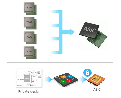
Key value of FPGA-Go-ASIC service
| Phase | Stage | Collaboration model | Customer |
Faraday |
|---|---|---|---|---|
| Design Phase | Customer's FPGA solution | Customer FPGA solution and market proven | ■ | |
| ASIC frot-end Design | HDL design translation from FPGA to ASIC | ◪ | ■ | |
| ASIC architecture evaluation: CPU, Bus, IP | ◪ | ■ | ||
| IP selection, configuration, customization | ◪ | ■ | ||
| SoC integration | ■ | |||
| SoC simulation, verification | ■ | ■ | ||
| FPGA Prototyping | FPGA hardware prototyping verification on Faraday’s prototyping platform | ◪ | ■ | |
| Software framework (OS, driver) porting | ■ | |||
| Application software function design | ■ | |||
| ASIC Back-end Design | Physical implementation | ■ | ||
| Post-layout, physical verification | ■ | |||
| Package design and testing | ■ | |||
| Engineering Sample Phase | Engineering Sample Verification | PCB spec. defining | ■ | |
| PCB system implementation | ■ | ■ | ||
| ASIC engineering sample verification | ■ | ■ | ||
| Application software and software Framework porting | ■ | |||
| Complete hardware and software system verification | ■ | ■ |
Success cases
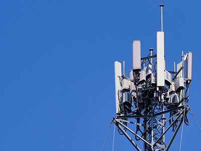 5G Wireless
+
5G Wireless
+
5G Wireless
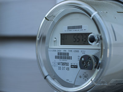 Smart Grid
+
Smart Grid
+
Smart Grid
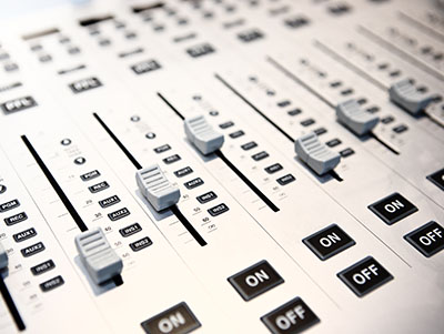 Audio Instrument
+
Audio Instrument
+
Audio Instrument
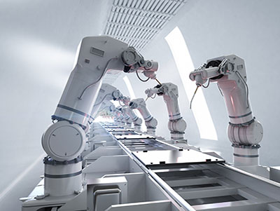 Industrial
+
Industrial
+
Industrial
 Customer Feedback
+
Customer Feedback
+
Customer Feedback
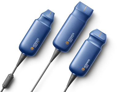
“Faraday technology has enabled EchoNous to provide clinicians around the world with previously unavailable ultrasound image quality and diagnostic options in a highly portable and low cost device.”
“The Faraday FPGA-to-ASIC path enables rapid product development and contributes greatly to first pass ASIC success.”
- Todd Willsie, VP of Hardware and Ultrasound Engineering at EchoNous