Compared to planar FET, FinFET brings the advantages of smaller size, higher performance, and lower leakage. With the fin shape channel, the gate can control drain-source channel in 3 sides and lead to a wider effective device width.

Challenges in FinFET Process
However, there are also some new challenges coming along with those advantages in FinFET process.
- Complex DRC rules caused by multiple pattering
- DFM requirements during implementation
- AOCV or POCV adopted to model process variations
- More STA sign-off corners
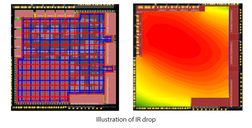
- IR/EM weakness
Based on the abundant ASIC experience and robust design capability, Faraday has developed its solutions for these challenges. To deal with the complex DRC rule, color aware is used in each stage; via swap and LPA flow are adopted to take care of the DFM rule during APR. AOCV/POCV is considered during physical implementation and timing ECO stage to ensure smooth timing closure. Meanwhile, less STA sign-off corners are checked to save run time.
Moreover, to solve the common issues of IR in FinFET process, Faraday has created an in-house tool, fera, which can analyze IR drop within about 20 minutes (for 2.5M instance count design) before placement. It enables the designer to detect IR weakness and improve the design in early stage.

Faraday's Design Flow on FinFET Platform
Faraday has built-up a solid, seamless, and efficient design flow to overcome these challenges in FinFET platform. It includes the synthesis, APR, timing closure, and physical verification stages. By this flow, we can implement a FinFET ASIC smoothly and quickly.
