System-in-package (SiP, or multi-chip module) is quite a hot topic in the competitive semiconductor industry. Especially on the ride of SoC trend, system-in-package is obviously a good solution for many size-sensitive applications. However, the technology has also brought new challenges to engineers not only in the packaging stage, but also from initial design to final testing, throughout the manufacturing processes. Based on abundant ASIC experiences, Faraday provides SiP design service to optimize customer's product performance, lower the cost, and further accelerate the time to volume.
Faraday SiP Design Flow

Faraday SiP flow consists of four stages:
1. Co-design stage
2. Package evaluation and design
3. ASIC implementation
4. Manufacturing and testing
Note: Stage 2 and 3 are simultaneous processes
Stacked Die Package
The stacked die package is the technology which stacks multiple dies vertically in the same package. This package can achieve higher density with smaller package size at the same time. Faraday provides the design service to combines Faraday's ASIC with other dies to reduce the cost and ensure the system performance.
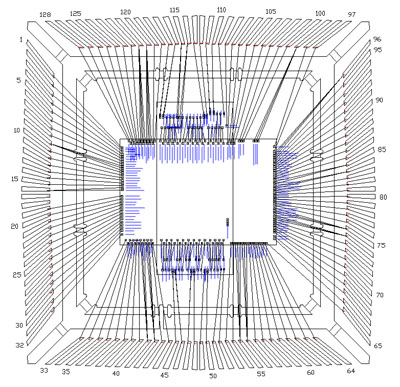
Example: timing-controller
Faraday's ASIC timing-controller design is assembled with a KGD (Known-Good-Die) in a QFP package with 128 pin counts. Faraday uses the internal tool to verify the bonding simulation, and determine the pad location and chip aspect ratio of the ASIC in one week.
Side by Side Package
Dies laid out side by side is another SiP technology with high cost-efficiency, taking both reliability and heat sink into consideration.
Side by Side + Stacked Die Package
Faraday provides not only side-by-side, or stacked die SiP solution, but also a single package with multiple dies adopting both side-by-side, and stacked technology together to achieve better performance.
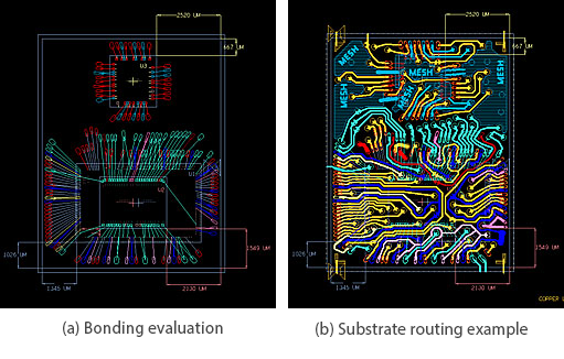
Example: GPS SiP Design
This case adopted TFBGA package with 116 pin counts with three dies inside, including Faraday's ASIC, flash and RF die. Faraday developed the BGA substrate including signal integrity analysis, power integrity analysis, IBIS model creation, and RLC extraction. Since the signals were very sensitive, Faraday performed signal integrity analysis to ensure the substrate routing to meet the customer's performance requirement.
SiP Interconnection Testing
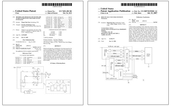
SiP die to die interconnection testing is challenging for these pins cannot be accessed from Automatic Test Equipment (ATE), as the following diagram shown.

However, the traditional testing methodologies only focus on solving the issue of single die but not the solution for multiple dies. Faraday has developed its two own KGD interconnection testing patents to solve the die to die testing issues, which were granted in 2007 and 2010.
- Built-in self-test for system in package Patent (Patent # 7,394,272)
- Method and apparatus of testing die to die interconnection for system in package patent application (Application #20100213965)
The first one is a function-dependent method, which implements a KGD BIST in ASIC die and use the BIST circuit to test the KGD functions and interconnection. The second one is function-independent method that is used for Flash type memory. It applies cap. measuring method to save the time for read/write/erase and can reduce the testing time from seconds to micro-second (10e-6sec).
These two patents were applied in many projects and successfully verified.
Success Cases
Faraday has implemented many SiP module projects successfully for various applications, including display, surveillance, GPS, and networking. The following table lists some of Faraday's success cases of SiP designs.
| Application | Package type | Component | Method |
|---|---|---|---|
| Display | EPAD-TQFP | ASIC+SDRAM | Stacked |
| Ethernet | LQFP | ASIC+Flash | Stacked |
| Ethernet | LQFP | ASIC+Flash | Stacked |
| Ethernet | LQFP | ASIC+Flash | Stacked |
| GPS | SQFN | ASIC+Flash | Stacked |
| GPS | TFBGA | ASIC+Flash+RF | Stacked+Side-by-side |
| GPS | TFBGA | ASIC+RF | Side-by-side |
| Multimedia | TFBGA | ASIC+SDRAM | Stacked |
| Surveillance | TFBGA | ASIC+SDRAM+Flash | Stacked+Side-by-side |
| T-Con | LQFP | ASIC+SDRAM | stacked |
| Wireless LAN | LQFP | ASIC+Flash | stacked |